owFabLiquid.
Three liquids. Three primitives silicon does not serve. One workcell.
OECT / iontronic. Liquid-metal reconfigurable. Reaction-diffusion. Fully mapped, fully realizable, fully vendor-sourced. On the shared Nano chassis, with the shared cartridge dock and the shared design surface.

Silicon does most things well.
It does not update weights at femtojoules per event. It does not rewire its own metal layer. It does not compute in parallel across a continuous medium. It does not talk to tissue without a transducer.
Three liquids that do.
Organic electrochemical transistors. Gallium-alloy reconfigurable interconnect. Chemical wavefronts in an excitable medium. Each one addresses a primitive class silicon has never served. Each one has a research group, a supply chain, and a workload that lives on it today.
One chassis, three substrates, one design flow.
Same 5-axis stage. Same cartridge dock. Same AI orchestrator. Aerosol-jet head prints PEDOT:PSS and eGaIn. A microfluidic cell holds the BZ chemistry. Camera-based readout closes the loop. Add DMF, physical reservoir, iontronic memristor, and DNA-storage cartridges as they arrive.
Fully mapped. Fully realizable.
Every substrate has a TRL read, a named research group, a vendor supply chain, a feature envelope, and a workload. Fifteen substrate families surveyed. Three primary, four secondary, seven excluded with reasons. The internal deep dive is 32 pages of engineering + market argument. Nothing hand-waved.
A design becomes a wet-side finished thing, in the room.
Silicon workloads, photonic workloads, liquid workloads. One design surface. One workcell family. One loop. In hours. Onshore. Wherever the design happens.
One chassis. Five head modules. Four cartridge families.
Top-view schematic of the shared Nano-class workcell with the wet-side additions loaded. Same 5-axis stage, same cartridge dock, same AI orchestrator, same enclosure and metrology bay used for silicon. Adding liquid substrates is head modules plus cartridge chemistry, not a new machine.
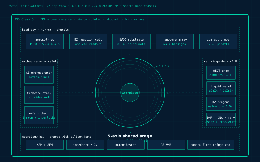
Three primary substrates. One cartridge dock.
Each one is a real primitive class silicon does not serve well. Each one has a real research group, a real supply chain, and a real workload today. Cartridge families for physical reservoir, digital microfluidics, iontronic memristors, and DNA-storage read/write add on the same chassis.
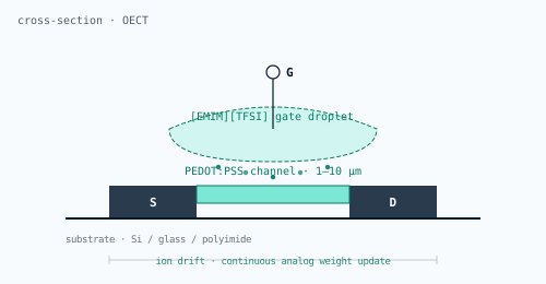
Wearable neuromorphic. Sub-100 fJ per weight update.
Organic electrochemical transistors update weights by ion drift, at less than 100 femtojoules per switching event. Printed at 1 to 10 micron feature scale by aerosol-jet PEDOT:PSS plus ionic-liquid gate. Native to the wet side of any biological interface, so the compute layer talks to tissue without a transducer.
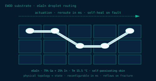
Reconfigurable RF. Millisecond topology change. Self-healing.
Gallium alloys (eGaIn, GaInSn) printed by aerosol jet or actuated across an electrowetting substrate. Physical topology IS the state. Reconfiguration in milliseconds. When a conductor breaks, surface tension reflows the metal and restores conductivity. Stretchable to five times length without electrical degradation.
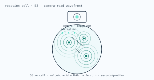
Spatial-parallel. The whole medium computes at once.
A Belousov-Zhabotinsky reaction cell in a microfluidic chamber. Chemical wavefronts propagate across the medium and interact by collision. Voronoi, Steiner tree, image skeletonization, and wave-based shortest path fall out of the collision physics without algorithmic encoding. Camera-based readout closes back into the design surface.
Every substrate has a research group, a vendor supply chain, and shipping chemistry. Not "could work in theory." Fifteen substrate families surveyed, three primary, four secondary, seven explicitly excluded with reasons.
Local-learning weight update, runtime topology change, spatial-parallel primitives, in-fluid biosignal transduction. Four primitive classes silicon does not serve well. Each mapped to the exact substrate that does.
Neural-interface companies, RF and space-hardened electronics primes, spatial-parallel research programs, DoD forward-deployment. Approximately 150 companies plus 60 university labs plus 25 defense-adjacent facilities at track launch.
Design in JLandauer. Fabricate in the room, across silicon, photonic, and now liquid substrates. Verify with in-situ metrology. Ship in hours instead of quarters. The loop that closed for silicon is the same loop, extended to the substrates silicon cannot reach.
Deeper.
Fully-mapped engineering + market + realizability argument. Every substrate, every head module, every cartridge, every BOM line, every named research group and vendor. Nothing here is speculative beyond what the substrate literature and vendor supply chain support today.
The board, the die, the liquid. One machine family. The desktop revolution reaching the thing that makes everything else.
The full multi-mode nanofab. 10 to 20 nm effective feature size. The shared chassis this liquid track lives on.
The design surface. Cloud IDE, MCP tooling, multi-PDK, and now multi-substrate. Speaks silicon, photonic, and liquid through one endpoint.
In development.
v0 bench prototypes underway. v1 track kit on the Nano chassis follows. We are sharing early with the research groups, cartridge OEMs, and forward-deployment programs building the wet-side.
Register interest →