OWFabricator / Nano.
Build chips in three dimensions.
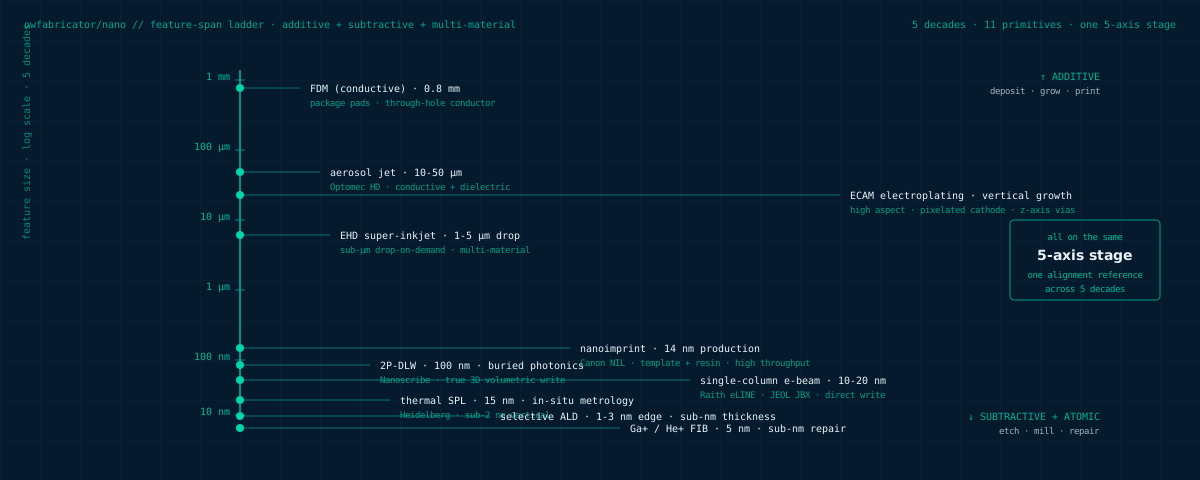
5-decade feature span. Eleven microscale primitives. One 5-axis stage. Additive + subtractive + multi-material — the same idea that made 3D printing work, at the tier the chip actually is.
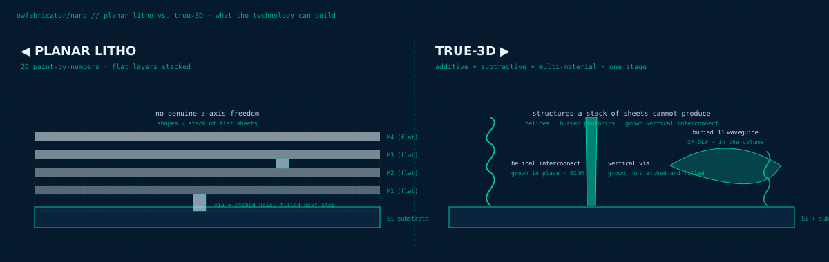
Planar lithography is 2D paint-by-numbers.
Vias are etched holes filled by the next step. Every layer is a fresh flat coat. There is no genuine z-axis. The structures the technology can build are the structures a stack of flat sheets can build. Nothing more.
A chip that is a 3D-printed object.
Treat microfabrication the way 3D printing already works — additive, subtractive, multi-material, on one moving stage — and the chip becomes an object. Helices. Buried optical waveguides. Vertical interconnect grown in place, not etched-and-filled. Shapes that planar litho was never meant to reach.
Eleven primitives. All shipping today.
Every microscale primitive we combine on the stage ships from a real vendor at production scale. Two-photon direct-write, aerosol jet, electrohydrodynamic super-inkjet, nanoimprint, electroplating, plasma ALE, selective ALD, thermal SPL, and more. Nothing here is a research prototype. The integration is the invention.
Five decades of feature size. One stage.
From 0.8 mm conductive FDM down to 100 nm two-photon DLW, all on the same 5-axis stage under the same ProcessGraph scheduler. The pipe from millimeter package pads to sub-micron device features never leaves the machine.
Design → fabricate → verify → iterate in hours.
Design in the openWafer surface. Fabricate on the stage. In-situ metrology verifies dimensions, alignment, and electrical continuity in place. The recipe adapts. The next iteration runs on the same stage. Onshore, wherever the design happens.
Planar litho vs. true 3D.
Planar photolithography treats fabrication as a stack of flat sheets — vias are etched holes filled by the next step, and every structure has to be one a stack of sheets can produce. True-3D fabrication grows the structure in place: helices, buried optical waveguides, vertical interconnect that never had to be etched. The technology decides what the chip can be, and the constraint changes with it.
Eleven primitives. One stage.
Every primitive in this list ships commercially today. The integration under one 5-axis stage, one scheduler, one cartridge dock, and one design surface is the invention.
Two-photon direct-laser-write. 100 nm feature scale for photonics, biomimetic structures, meta-optics.
10-20 nm direct-write electron-beam lithography for template pre-fab and one-off nanoelectronics.
Template-based printing at 14 nm production, 10 nm via replica templates. High-throughput.
Conductive ink deposition at 10-50 µm for interconnect and printed electronics.
Electrohydrodynamic jet for sub-micron drop-on-demand — conductive + dielectric + photonic.
Atomic-layer deposition with SAM/SMI inhibitors. Sub-nm thickness + 1-3 nm feature-edge control.
Pixelated-cathode electroplating for high-aspect-ratio vertical structures grown in place.
Atomic-layer etch for controlled subtractive patterning. Complement to selective ALD.
15 nm lateral + sub-2 nm vertical scanning-probe lithography with in-situ metrology.
5 nm milling with Ga+, sub-nm with He+. Point-defect repair, cross-sectioning, direct patterning.
In-workcell bonding head for 3D stack assembly. Same alignment reference as every prior step.
0.8 mm FDM through 100 nm 2P-DLW on the same stage. The pipe from package pad to device feature never leaves the machine.
Genuine z-axis freedom. Helices, buried photonics, vertical interconnect grown in place. Structures planar litho cannot reach.
Deposit, etch, plate, cure, image — all on one stage. Multi-material where the design needs it, mono-material where it doesn't.
What becomes possible.
Piezo transducer layers stacked vertically with grown-in-place interconnect. Structures a stack of flat sheets cannot produce.
Waveguides written into the substrate volume with 2P-DLW. Curves, crossovers, 3D vertical couplers — geometries planar photonics cannot draw.
Translinear cells stacked vertically, grown in place. Log-math primitives at densities planar-analog layout cannot reach.
Design in JLandauer. Fabricate on the stage. Verify with in-situ metrology in place. Adapt the recipe and re-fab — process design at the speed of software. In hours, onshore, wherever the design happens.
Deeper.
The board, the die, the liquid. One machine family. The desktop revolution reaching every part of the electronics stack.
The whole SMT line — print, drill, dispense, place, reflow, inspect — on one 5-axis stage. Sibling technology to Nano.
OECT, liquid-metal, reaction-diffusion. Wearable neuromorphic, reconfigurable RF, spatial-parallel primitives.
In development.
Plan of record set. We are sharing early with the specialty-silicon customers who want to build the structures planar fabrication cannot reach.
Register interest →