OWFabricator / PCB.
Make the whole board, on your bench.
The whole SMT line — print, drill, dispense, place, reflow, inspect — on one 5-axis stage. Enclosed, cartridge-fed, in the room. Clean, onshore, in hours.
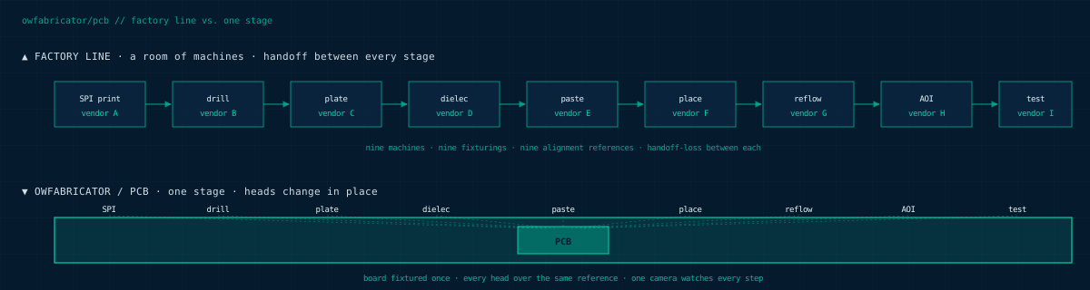
A factory line is a mile of conveyors.
Print, drill, dispense, place, reflow, inspect — every step is a different machine, a different vendor, a different fixturing standard. The board moves through the line and every handoff is a chance to lose it. That is why prototyping a PCB still means shipping files to a fab a week away.
The same primitives, one stage.
Every SMT primitive shipping in the factory works on a single 5-axis stage. Fixture the board once. The heads move over it. One camera watches. One workflow decides what happens next. The factory's proven reliability at the scale of a single board.
Enclosed. Cartridge-fed. In the room.
Solder paste, conductive ink, encapsulant, solvent, waste — every consumable is a cartridge you plug in. The scrubber captures every fume. The enclosure keeps the operator out of the process and the process out of the room. Standard wall power, standard shop air.
Additive by design. Nothing dumped.
The process is additive where it can be, subtractive where it must be, and closed-loop everywhere. Copper is printed and sintered, not etched. Solder mask is dispensed and cured, not stripped. Waste is captured in the cartridge, not the drain. Green because of how it works, not in spite of it.
A design becomes a tested board, in the room.
Design in JLandauer or the openWafer surface. Fabricate on the stage. Inspect with the same camera that watched every step. Test in place. Iterate in hours. Onshore, wherever the design happens.
A factory line, collapsed to one stage.
Top row: a traditional SMT factory line — nine separate machines from nine vendors, nine fixturings, nine alignment references, a handoff cost between each. Bottom row: the same functional stages compressed onto one 5-axis stage with a single fixturing and one camera reference. Every handoff a factory line pays for is eliminated by fixturing once.
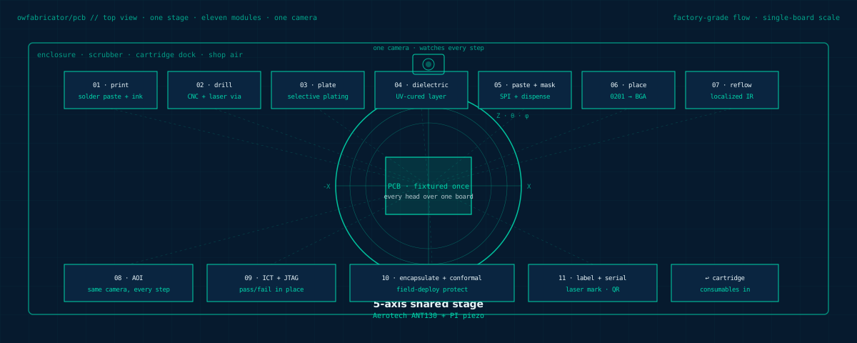
Eleven modules. One stage.
Each of the machines a factory SMT line pipelines becomes a head on the 5-axis stage. Board fixtured once. Heads change in place. Camera watches every step. Same alignment across every operation.
Solder paste and conductive-ink deposition through direct-write jets. Sub-100 µm dots on demand.
CNC micro-drill for through-holes and vias, plus laser drill for microvias down to 50 µm.
Selective electroless plating for via barrels + trace conductivity. Immersion + rinse in cartridge chemistry.
UV-cured dielectric layer deposition for multi-layer stack-ups. Thickness controlled per pass.
Solder mask + selective solder paste dispense, aligned to the pad map with the stage-mounted camera.
0201 through BGA, tape + tray + waffle input, vision-aligned placement to 25 µm.
Localized IR reflow head — heats only the assembly region. No oven, no thermal shock to the whole board.
Automated optical inspection after every step. Same camera. Same alignment. No separate machine.
Bed-of-nails or probe-card in-circuit test, plus JTAG boundary-scan. Pass/fail in place.
Conformal coating and localized encapsulation dispense for field-deploy boards.
Laser-mark serial + QR + barcodes on the finished board. Same stage.
The SMT print → place → reflow → inspect → test pipeline runs in production every day at industrial scale. The OWFabricator brings that same flow onto one stage.
Every head over one board that never moves. One camera. One alignment reference. Every handoff a factory line pays for is eliminated by fixturing once.
Additive where it can be. Copper printed and sintered, not etched. Solder mask dispensed, not stripped. Waste captured in cartridges, not dumped.
Design in JLandauer. Fabricate on the stage. Inspect with the same camera that watched every step. Test in place. Iterate in hours. The board leaves finished, wherever the design happens.
Deeper.
The board, the die, the liquid. One machine family. The desktop revolution reaching every part of the electronics stack.
The full multi-mode nanofab. 10 to 20 nm effective feature size on additive + subtractive primitives.
OECT, liquid-metal, reaction-diffusion. Wearable neuromorphic, reconfigurable RF, spatial-parallel primitives.
In development.
Plan of record set. We are sharing early with the labs, startups, and defense forward-deploy teams that want a factory-grade PCB workcell on their bench.
Register interest →